FLYING PROBE TESTER
FA1283
a Single Unit
|
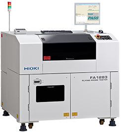
Hioki PCB and substrate inspection equipment leverages our core competency in high precision component testing. The FA1283 is a horizontal-loading, double-sided flying probe tester with a minimum 15 μm × 15 μm probing precision and rapid 100 times/second test speed. Key Features |
Model No. (Order Code)
|
|
Complete Electrical Testing of High-Function Boards with a Single Unit The FA1283 is a next-generation bare board testing system that incorporates component measurement expertise accumulated by Hioki in the course of developing populated board testing products. |
|
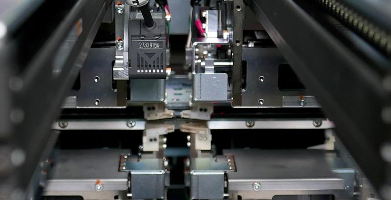 |
Down to the 1μm A High-Accuracy FLYING PROBE TESTER Aiming at φ10 μm Contact Total Probing Accuracy □ 15 μm (when FA1971-01 is installed) |
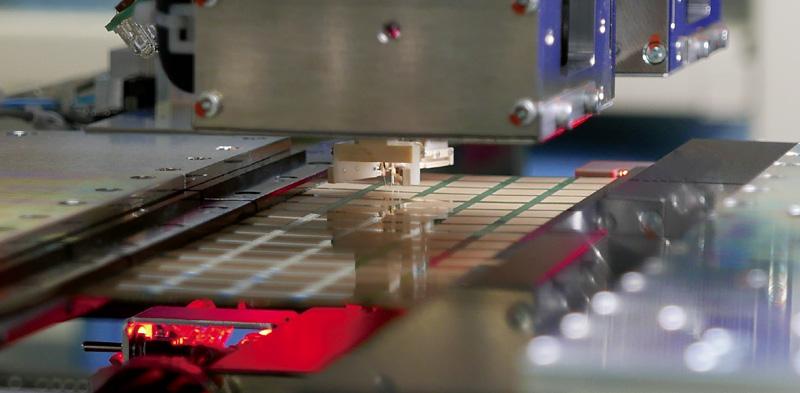 |
Not One Second Wasted A smooth start to initial testing is vital. |
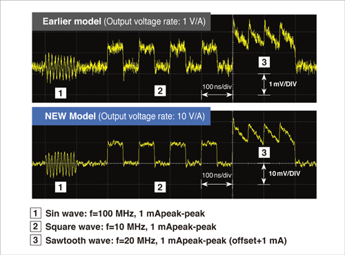 |
Total Measurement Mastery A single unit for everything from simple continuity and insulation testing to advanced function measurements for component testing. |
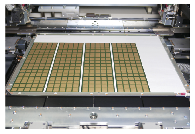 |
Vacuum Unit for Capacitance Test E4001 “Nothing ships without electrical testing.” |
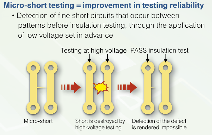 |
Improving the quality of insulation testing The tester’s insulation test capabilities have a direct impact on product quality when it comes to phenomena such as burning up micro-shorts and arcing during testing. |
 |
Mastering continuity testing and resistance measurement Users can select from multiple modes, including 4-terminal low-resistance measurement, 200 mA continuity measurement, and capacitance measurement O/S testing. |
|
Embedded Device Measurement: A Sharp Departure from LCR Measurement The FA1283 is a next-generation bare board testing system that incorporates component measurement expertise accumulated by Hioki in the course of developing populated board testing products. These functions are ideal for testing populated boards and differ from those offered by LCR meters. |
|
 |
Half of Data Generation Time With New Platform FEB-LINE UA1781 Flying probe test for Embedded and Bare boards UA1781 ・3-in-1 for editing, test-point generation, and built-in component support |
Specifications Overview
| Number of arms | 4 (2 each, top and bottom) | |
|---|---|---|
| Mountable probes | 1172 series | |
| Number of test steps | Max. 900,000 steps | |
| Measurement parameters and measurement ranges | Resistance : | 40.00 μΩ to 100.0 MΩ |
| Capacitance : | 10.00 fF to 40.00 mF | |
| Inductance : | 10.00 μH to 100.0 mH | |
| Diode VZ measurement : | 0.000 V to 25.00 V | |
| Insulation resistance : | 200.0 Ω to 100.0 GΩ | |
| Capacitance Insulation resistance : | 200.0 Ω to 10.00 MΩ | |
| High voltage resistance : | 200.0 Ω to 25.00 GΩ | |
| High voltage short resistance : | 400.0 mΩ to 400.0 kΩ | |
| Leak current measurement : | 100.0 nA to 10.00 mA | |
| Zener diode VZ measurement : | 0.000 V to 25.00 V | |
| Digital transistor measurement : | 0.000 V to 25.00 V | |
| Photo couplers measurement : | 0.000 V to 25.00 V | |
| Continuity test : | 400 mΩ to 1.000 kΩ | |
| Open test : | 4.000 Ω to 4.000 MΩ | |
| Short test : | 400.0 mΩ to 40.00 kΩ | |
| DC voltage measurement : | 40.00 mV to 25.00 V | |
| Judgment range | -99.9% to +999.9% or absolute value | |
| Overall probing precision | 20 μm (Square)/ 15 μm (Square) (when using FA1971-01) | |
| Measurement time | Max. 100 points/ s (X-Y movements of 0.1 mm, 2-arm simultaneous probing, when capacitance measurement) | |
| Testable board size | Thickness : 0.1 mm to 2.5 mm (0.10 in) Outer dimensions : 50 mm (1.97 in) W × 50 mm (1.97 in) D to 400 mm (15.75 in) W × 330 mm (12.99 in) D |
|
| Maximum testable area | 400 mm (15.75 in) W × 324 mm (12.76 in) D | |
| Board clamping | Board 2-side chuck method (with tension function) | |
| Power supply | 200 V, 220 V, 230 V, 240 V AC single-phase (specify upon order), 50/60 Hz, 5 kVA | |
| Dimensions and mass | 1360 mm (53.54 in) W × 1200 mm (47.24 in) H × 1280 mm (50.39 in) D, (Excluding protruding parts), 1,100 kg (38,800.7 oz) | |

