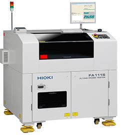
FLYING PROBE TESTER
FA1116
the Impact Mark Depth
|
The Flying Probe Tester FA1116-03 is a high-speed automatic board tester that uses newly developed low-impact probes and precision soft-landing control to achieve 30% faster cycle times for gold plating and fine pattern testing than legacy products. Key Features |
Model No. (Order Code)
|
 |
HIOKI ATE LINEUP [ The Power to Connect ] The power to connect that Hioki’s printed circuit board testing systems deliver is the power to connect to the future. The ability to continue to support this rich and satisfying lifestyle together with customers is a small part of what testing systems can do. |
|---|---|
 |
Information movie FA1116
|
 |
Advantages of capacitance testing Capacitance testing is an essential test technique for reducing flying probe test times. The greatest advantage of the vacuum-clamp method is that testing can be carried out without regard to the board shape or the number of layers.Products cannot be shipped unless they can be verified to be non-defective through testing. The ability to test various boards is the top priority for a tester. Test times are determined by the number of test points and the speed setting, which reflects the extent of impact marks. |
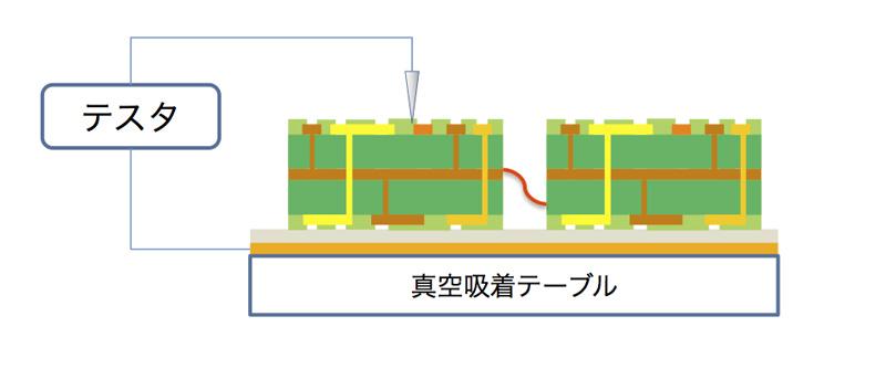 |
Advantages of single-sided vacuum-clamp capacitance testing (discontinuity testing) Single-sided testing is characterized by the ability to conduct continuity testing with other nets. |
 |
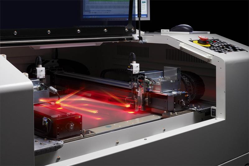
Stable impact marks and high-speed testing To the extent that electrical testing is performed, probe impact marks on the circuit board are inevitable.It goes without saying that a fixed set of conditions can be easily identified for the tester if the measurement target conforms to certain fixed conditions itself. |
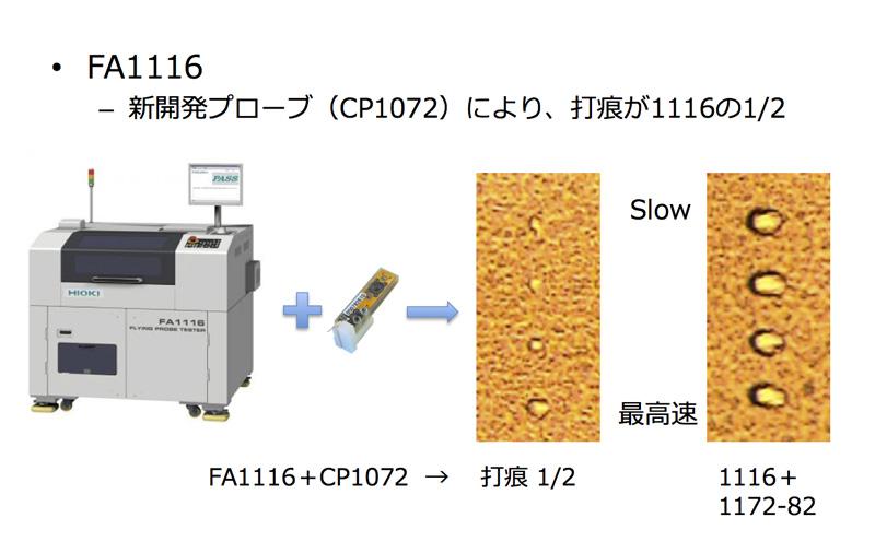 |
Reduced-impact link probes (option) By combining newly designed reduced-impact probes and precision soft-landing control, the FA1116-03 makes it possible to approach the maximum speed setting during fine pattern testing. |
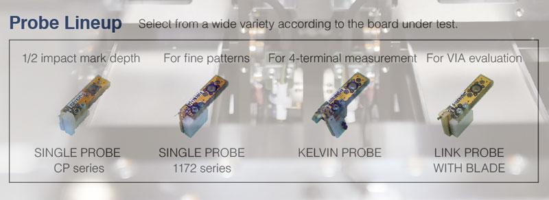 |
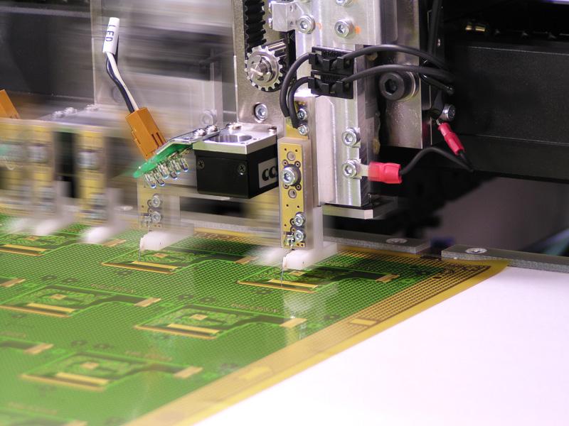
Probe lineup Users can select from an extensive range of variations based on the types of boards they wish to test. |
 |
Edit Gerber data with the FEB-LINE UA1781. In the UA1781 data creation system, Hioki developed its own software for editing Gerber data. |
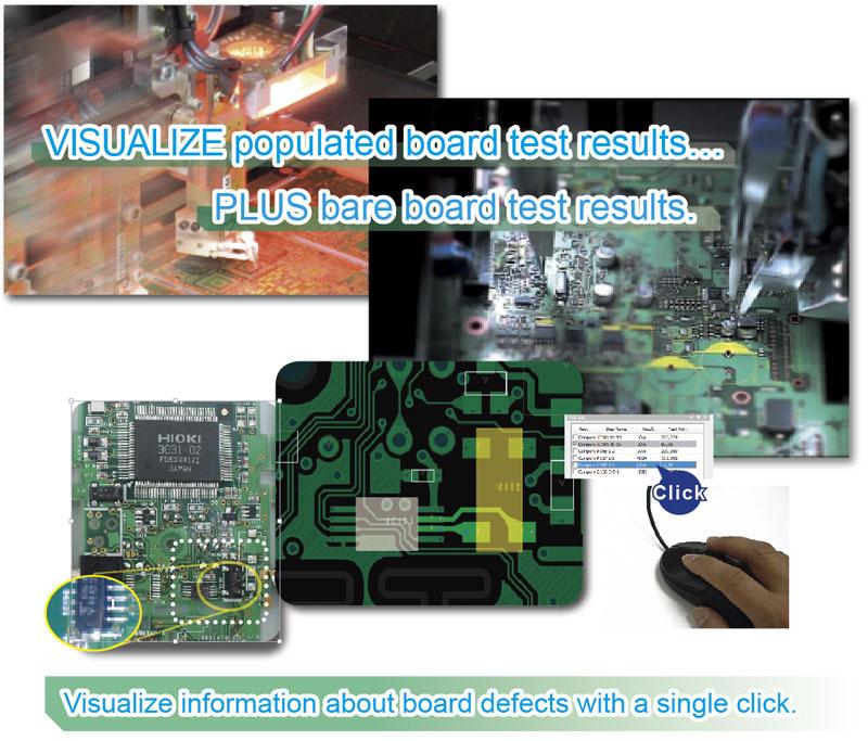 |
Search for defective nets with the FAIL VISUALIZER UA1782. Viewer software that displays defective nets and searches for defect locations based on the results of capacitance measurement. |
Specifications overview
| Number of arms | 2 |
|---|---|
| Number of test steps | Max. 40,000 steps/piece 300,000 steps/sheet |
| DC Measurement ranges | Resistance : 400 μΩ to 40 MΩ Capacitance : 4 μF to 40 mF Diode, transistor (VF) : 0 to 25 V Zener diode (VZ) : 0 to 25 V Short :400 mΩ to 40 kΩ Open :4 Ω to 4 MΩ Voltage :0 to 25 V |
| AC Measurement ranges | Resistance : 100 Ω to 100 MΩ Capacitance : 10 fF to 10 μF Inductance : 10 μH to 100 mH |
| Measurement time | Max. 100 points/s (X-Y movements of 0.1 mm, 2 arm simultaneous probing, capacitance measurement) |
| Probe working area | 610 mm (24.02 in) W × 510 mm (20.08 in) D |
| Fixed board dimensions | Thickness : 0.1 mm to 3.2 mm (0.13 in) Outer dimensions : 50 mm (1.97 in) W × 50 mm (1.97 in) D to 610 mm (24.02 in) W × 510 mm (20.08 in) D Upper surface – 10 mm (0.39 in) (including board thickness) Lower surface – 0.1 mm (0.00 in) |
| Board-carrier | N/A |
| Power supply | 200 V AC ±10% (single-phase), 50/60 Hz, 3 kVA |
| Dimensions and mass | 1,443 mm (56.81 in) W × 1,656 mm (65.20 in) H × 1,185 mm (46.65 in) D, 1,000 kg (35,273.4 oz) |
